How does a printed circuit board fabrication work?
Printed
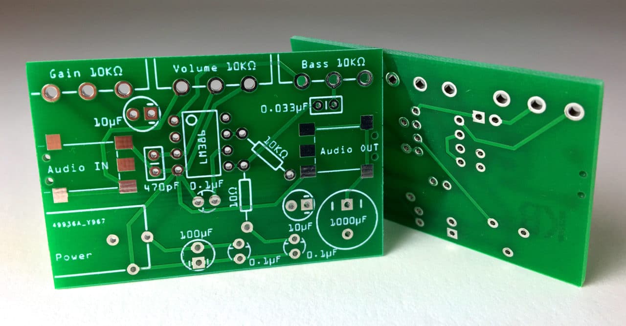
Circuit Boards (PCBs) are the backbone of all electronics industry. The PCBs
are used in almost all the inventions of electronics, which include
calculators, digital clocks, and all other devices. These circuit boards are
called backbone because they teach the electricity where to flow and give life
to all electronics. It satisfies the requirements of the mechanical and
electrical circuit of the device.
Printed
board circuits pass current in the region of the surface via the set of
connections of copper pathways. The complicated system of connections of copper
pathways explains the inimitable role of the printed circuit board.
PCB
manufacturing process includes steps which are as follows:
Design of PCB and output
The most
important thing you need to have before you start the manufacturing of the PCB
board is a good design for the board. So, the first step for PCB manufacturing
is choosing a suitable design for it. You can make it easy for you to select a
design by using automated software for it. You can use a trace width calculator
to keep track of all minor details related to external and inner layers and
ensure that the design of the PCB perfectly fits your needs and requirements.
Conversion
of the file to film
The next
step is to print the finalized design of the PCB. For this purpose, a special
printer is used, which is termed is plotted printer. Two colors of ink are used
as it helps to differentiate between the conductive and non-conductive areas.
You can visit https://www.pcb-togo.com/ to read more about Printed Circuit boards and
its functions. The same colors are used on the outer layers and inside layers
of the board, but their meaning is different in each one of them.
Remove
unwanted copper and inspect it

There are
several steps involved in the manufacturing of a PCB, but one of the most
important ones is removing the unwanted copper and then inspecting it
thoroughly. You can use an alkaline solution for removing the copper as it will
consume all the extra copper from the board without harming any other part.
Once unwanted
copper is removed, you need to inspect it properly for the alignment of outer
and inner layers. It helps to ensure that there are no issues on the board as
after this stage, it will be impossible to correct any error.


Comments
Post a Comment